Design and Measurement of CMOS RF-DC Energy Harvesting Circuits
Presenter: Dr. Murat Eskiyerli, Revolution Semiconductor
Date: Tuesday, May 3, 2016
Time: 1:00pm to 4:30pm
Venue: S331-A
This tutorial starts from the first principles and covers the single and multi-stage CMOS RF to DC rectifier design, efficiency, the simulation methodology and the measurement methods for the chip input impedance — a prerequisite for the design of the optimum tag antenna.
Topics
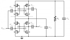 The requirements for RF energy harvesting circuits
- RF Rectifier Circuits
- Diode-C Rectifier Rectifier
- Diode-connected MOSFET-C rectifier circuit
- Differential-drive CMOS rectifier circuit
- Power Conversion efficiency (PCE) and output voltage of CMOS Rectifier
- Design of Multi-stage (cascaded) CMOS rectifier circuits.
- Selection of the number of stages in a rectifier block.
- Avenues for further optimization of CMOS rectifier circuits.
- Rectifier Input Impedance of Simulation and Measurement
- The need for determination of the input impedance of the rectifiers
- Inadequacy of the conventional small-signal analysis and simulations
- The simulation methods
- Transient Simulation methods
- Shooting-Newton type simulations
- The determination of the actual RF input power from simulations
- The characteristics of the input current/voltage in time and frequency domains
- Quick and accurate testbench measurement of the input impedance
- Optimization of the input impedance of the RF rectifiers.
Speaker Biography
 Dr. Eskiyerli received BS degree in Electronic Engineering from Bogazici University, Istanbul in 1990 and MS Degree in Electrical Engineering from Case Western Reserve University, Cleveland, Ohio in 1992. He finished his PhD at Imperial College London in 1997. He has worked for various US and UK semiconductor companies, e.g. Sony Semiconductor, National Semiconductor, Analog Devices and Cambridge Silicon Radio (now Qualcomm). In 2010, he founded the Revolution Semiconductor in Ankara, Turkey specializing on ultra-low power RFIC design.


